VHDL-based FPGA development for the micro-line C6412Compact DSP / FPGA platform.

enables development of customized FPGA designs
contains VHDL framework for completely new designs
contains micro-line busmaster FPGA design as starting point for new designs
IP cores for operation of the IEEE1394 chipsets included
UART IP core included
configurable EMIF interface included as source code
documentation of all components included
Timing simulation available as an option


The FPGA Development Package
The FPGA development package gives the user the possibility to add virtually any kind of hardware to the C6412Compact. Interfaces not supported by the C6412Compact can be added by an appropriate FPGA design. Communication between DSP and external hardware can be optimized to perfectly fit the connected components. Data transfer overhead between DSP and FPGA can be minimized using different methods, such as a FIFO buffering, direct SDRAM access by the FPGA or implementaiton of PDT transfers. High speed signal processing, such as decimation filters, etc. can be moved from DSP software to the FPGA, relieving the DSP. The FPGA can also be used to interact with the DSP's on-chip interfaces such as accessing the DSP's HPI, triggering EDMA transfer over the GPIO lines or acting as a bus arbiter for PCI host oparation.

Spartan-3 FPGA Technology
The C6412Compact supports the upper end of the Spartan-3 FPGA family of devices, starting from 1Mgates (device type XC3S1000) up to 5Mgates (XC3S5000). The Spartan-3 device family is a successor of the earlier, successful Spartan-IIE family, equipped with more logic resources, more memory capacity and improved clock management, optimized for high performance at low cost. Some key features of these devices (shown for an XC3S4000 device) are:
- 192 Kbyte block RAM
- 622+ Mbps data rate per I/O
- 4 Digital Clock Managers (DCM) for clock de-skew, frequency synthesis, etc.
- 96 dedicated 18x18 hardware multipliers

A Rich Set of Resources
On the C6412Compact, the user benefits from a rich set of resources. Connection to the DSP's external memory interface (EMIF) provides the default link between hardware data processing in the FPGA and software data processing in the DSP. The EMIF can be operated in different ways:

  • using a register-based interface where the DSP accesses FPGA registers which are mapped into the DSP's address space. Accesses are done by software of over the DSP' s EDMA controller.
  • using PDT transfers, which are a special kind of EDMA transfer using single-cycle, busmaster-like transfers
  • using busmaster operation where the FPGA arbitrates for the EMIF and autonomously accesses the SDRAM
Alternatively the FPGA can access the DSP over its on-chip interfaces. This provides a completely independent data path to the CPU and therefore leaves the EMIF free for other purposes, such as DSP to SDRAM transfers. In default hardware configuration of the C6412Compact, the HPI16 interface can be used and the FPGA must implement 16-bit host port master operation. For the other configurations (HPI32 and PCI), the FPGA must implement 32-bit host port master or PCI host operation.

Different clock sources eliminate the need for external clock oscillators. Available are:

  • 120 MHz EMIF clock
  • 60 MHz EMIF clock divided by 2
  • 44.2368 MHz UART clock
  • 24.576 MHz clock from the IEEE1394 chipsets
  • 25MHz Ethernet clock or 33 MHz PCI clock (depending on board configuration), hardware modification may be necessary.

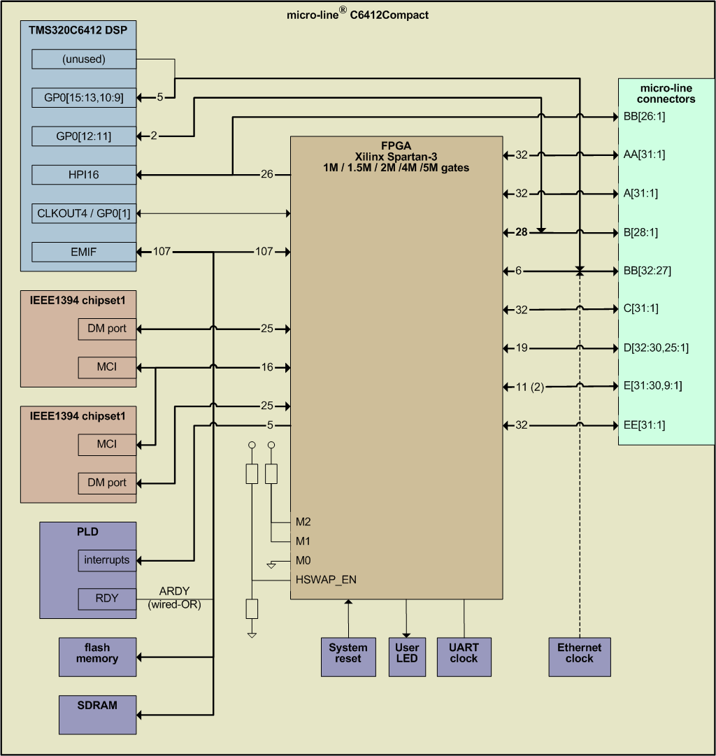
Up to 218 FPGA I/O connections to the micro-line connectors gives enough I/O capability for implementing multiple external interfaces. Most of these I/O resources can be used freely for own FPGA designs. The block diagram below shows the wiring of the FPGA for a C6412Compact in standard configuration (HPI16 & Ethernet).

micro-line Busmaster BSP FPGA Design Included
The micro-line busmaster FPGA design acts as a peripheral to the DSP where slow peripherals are accessed with asynchronous accesses and fast peripherals are accessed with synchronous burst accesses. It provides a well qualified starting point for own designs. This design is provided as development project, including VHDL source code and the necessary IP cores. Reliability of this design is guaranteed by timing constraints and can further be verified by timing simulation. A previously recorded simulation run of the micro-line busmaster FPGA design serves as a reference. For customization, existing function blocks can easily be removed and new function blocks can be added.

Alternatives to the micro-line Busmaster BSP
The micro-line busmaster BSP is a good starting point for quick and easy setup of completely customized FPGA designs and for customized FPGA designs that use at least a part of the BSP's features However, when adding more and more function blocks to the existing design, timing gets more and more critical, espacially for adress decoding between the function blocks. For such situations, alternative approaches using a single FIFO interface or block memory should be considered. Application note XAPP753 from Xilinx shows some examples.

Development Tools
The default development environment is Xilinx ISE. It provides the complete design process from code entry to programming file generation and FPGA configuration. The smaller two FPGA devices (XC3S1000 and XC3S1500) are supported by the free WebPack version of Xilinx ISE. For timing simulation, an optional timing simulation pacakge is available which requires ModelSim. For simulation of smaller designs, the starter version of ModelSim XE can be used. For simulation of larger and complex designs the full version of ModelSim XE is recommended. After development has finished, the FPGA can be configured by different methods:
- direct configuration over JTAG
- automatic configuration on startup by the C641xCPU's Flash File System
- application software controlled configuration from flash memory or RAM

Technical Data

The FPGA Development Package includes:

 
micro-line busmaster BSP The default FPGA for the micro-line C6412Compact, as included in the software development kits.

Implements access to the IEEE1394 chipsets, a peripheral interface, an auxiliary UART, configurable clock outputs and programmable LED control.

Provided as an ISE project, separately for each device.
VHDL framework Defines all available FPGA connections

Available for each hardware configuration of the C6412Compact

Synthesizable VHDL top-level entity
IEEE1394 IP cores Common IP core for FIFO buffered, 64-bit wide access to the register interface of both IEEE1394 chipsets.

FIFO buffered, 64-bit wide access to streaming data over a dedicated interface of the IEEE 1394 chipsets, separate for each chipset and each transfer direction.
UART IP core FIFO buffered UART IP core with programmable baud rates.
Simulation suport Recorded simulation sessions included for reference.

Timing simulation with ModelSim available as an option
Documentation FPGA Programming Guide

Streaming cores user's guide

UART IP core user's guide
 

For more information about the
FPGA Development Package
and pricing details:

Click here


Back to the C6412Compact product page:

Click here