VHDL-based FPGA development for the micro-line C6713Compact-2 DSP / FPGA platform.

Enables development of customized FPGA designs
Contains VHDL framework for completely new designs
Contains micro-line busmaster FPGA design as starting point for new designs
IP core for operation of the IEEE1394 chipset included
IP core for DDR3 memory access included
Documentation of all components included


The FPGA Development Package
The FPGA development package gives the user the possibility to add virtually any kind of hardware to the C6713Compact-2. Interfaces that are not supported by the C6713Compact-2 can be added by an appropriate FPGA design. Communication between DSP and external hardware can be optimized to perfectly fit the connected components. Data transfer overhead between DSP and FPGA can be minimized using different methods, such as a FIFO buffering or direct SDRAM access by the FPGA. High speed signal processing, such as decimation filters, etc. can be moved from DSP software to the FPGA, reducing CPU load on the DSP. The FPGA can also be used to interact with the DSP's on-chip interfaces such as accessing the DSP's HPI or triggering EDMA transfers.

Spartan-6 FPGA Technology
The C6713Compact-2 supports the upper end of the Spartan-6 FPGA family of devices, starting from LX45 (equals 43661 logic cells) up to LX150 (147443 logic cells). Some key features of these devices (shown for an LX45 device) are:
- 261 Kbyte block RAM
- Up to 1,080 Mb/s data transfer rate per differential I/O
- 4 clock management tiles (2 DCMs, 1 PLL each)
- 58 DSP48A1 slices for signal processing
- Memory controller blocks (MCBs) for easy connection of DDR memory devices

A Rich Set of Resources
On the C6713Compact-2, the user benefits from a rich set of resources. Connection to the DSP's external memory interface (EMIF) provides the default link between hardware data processing in the FPGA and software data processing in the DSP. The EMIF can be operated in different ways:

  • using a register-based interface where the DSP accesses FPGA registers which are mapped into the DSP's address space. Accesses are done by software or over the DSP' s EDMA controller.
  • using busmaster operation where the FPGA arbitrates for the EMIF and autonomously accesses the SDRAM
Alternatively the FPGA can access the DSP over its host port interface (HPI). This provides a completely independent data path to the CPU and therefore leaves the EMIF free for other purposes, such as DSP to SDRAM transfers.

Boards with LX75 FPGA or higher have access to 256 Mbytes of dedicated DDR3-800 memory. A predefined core from Orsys provides the necessary infrastructure and implements a single, 32-bit wide bi-directional DDR3 memory port for FPGA-designers.

Different clock sources eliminate the need for external clock oscillators. Available are:

  • 100 MHz EMIF clock
  • 150 MHz from DSP
  • 25 MHz from DSP
  • 24.576 MHz data mover clock from the IEEE1394 chipset
  • 11.0592 MHz UART clock from the PLD
  • 8 kHz cycle clock from the IEEE1394 chipset

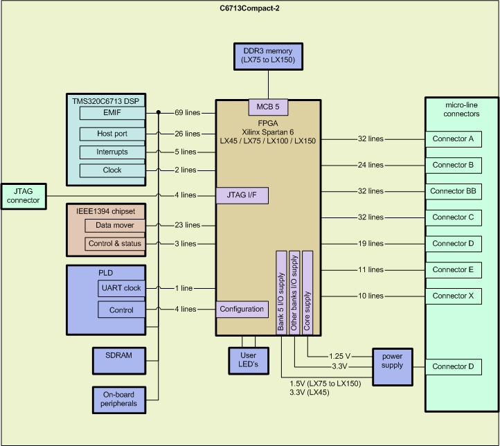
Up to 160 FPGA I/O lines to the micro-line connectors provide enough I/O resources for implementing multiple external interfaces. Most of these I/O connections can be used freely by the customer. The block diagram below shows the wiring of the C6713Compact-2 FPGA.

micro-line Busmaster BSP FPGA Design Included
The micro-line busmaster FPGA design acts as a peripheral to the DSP adding the following function blocks:

  • a peripheral interface with programmable timing for accessing peripheral boards over the micro-line bus
  • configurable clock output as part of the peripheral interface
  • interrupt control for internal and external interrupt sources
  • access to the data mover port of the IEEE1394 chipset for software-based data streaming
  • control of two user-programmable LEDs
The micro-line busmaster FPGA design provides a well qualified starting point for own designs. It is provided in the kit as development project, including VHDL source code and the necessary IP cores. Reliability of this design is guaranteed by timing constraints and can further be verified by timing simulation using Xilinx Isim. For customization, existing function blocks can easily be removed and new function blocks can be added. A modified version of the micro-line busmaster FPGA is also included, showing a simple implementation of DSP-based DDR3 memory accesses.

Alternatives to the micro-line Busmaster BSP
The micro-line busmaster BSP is a good starting point for quick and easy setup of completely customized FPGA designs and for customized FPGA designs that use at least a part of the BSP's features. When adding more and more function blocks to the existing design, timing gets more and more critical, especially for address decoding between the function blocks. For such situations, alternative approaches using a single FIFO interface or block memory can be considered. Application note XAPP753 from Xilinx shows some examples. Designs that completely differ from the micro-line busmaster BSP can be created from scratch using the VHDL framework provided.

Development Tools
The default development environment is Xilinx ISE. It provides the complete design process from code entry to programming file generation and FPGA configuration. Simulation is also supported by Xilinx Isim, which is included in Xilinx ISE. A free version of the ISE tools called WebPack is also available, limited to the smaller two FPGA devices (LX45 and LX75) and using a performance-limited version of Isim. After development has finished, the FPGA can be configured by different methods:
- direct configuration over JTAG
- automatic configuration on startup by the C6713Compact-2's Flash File System
- application software controlled configuration from flash memory or RAM

Technical Data

The FPGA Development Package includes:

 
micro-line busmaster BSP The default FPGA for the micro-line C6713Compact-2, as included in the software development kits.

Implements access to the data mover port of the IEEE1394 chipset, a peripheral interface, configurable EMIF clock output and user LED control.

Provided as an ISE project, separately for each device.
Timing simulation provided by Isim scripts.
VHDL framework Defines all available FPGA connections
Synthesizable VHDL top-level entity
IEEE1394 IP core IP core for FIFO buffered, 32-bit wide access to streaming data over a dedicated interface of the IEEE 1394 chipset (data mover port)
DDR access core MCB core implementation, customized for C6713Compact-2.
400MHz operation (DDR3-800)
Single-port, 32-bit wide, bi-directional interface.
Simulation support Scripts for timing simulation of the micro-line busmaster BSP

Simulation model for asynchronous DSP EMIF

Simulation model for IEEE1394 chipset's data mover port

Simulation model for a micro-line peripheral component
Documentation FPGA Programming Guide

Streaming IP core user's guide
 

For more information about the
FPGA Development Package
and pricing details:

Click here


Back to the C6713Compact-2 product page:

Click here